
Cables are ubiquitous in electronic-based systems. Electromagnetic emission of cables and crosstalk between wires is an important issue in electromagnetic compatibility and is to be minimized in the design phase. To facilitate the design, models of different complexity and accuracy, for instance, circuit models or finite element (FE) simulations, are used. The purpose of this study is to compare transmission line parameters obtained by measurements and simulations.
Transmission line parameters were determined by means of measurements in the frequency and time domain and by FE simulations in the frequency domain and compared. Finally, a Spice simulation with lumped elements was performed.
The determination of the effective permittivity of insulated wires seems to be a key issue in comparing measurements and simulations.
A space decomposition technique for a guided wave on an infinite configuration with constant cross-section has been introduced, where an analytic representation in the direction of propagation is used, and the transversal fields are approximated by FEs.
1. Introduction
One main goal of the present work is to match measurement data, Spice (LTSpice, 2020) and finite element (FE) simulations to create models of different complexity. A configuration as simple as a single insulated wire above ground needs to be modeled, built and tested to extract the equivalent RLGC-parameters, characteristic impedance Z0, velocity factor vf, as well as delay time td. Naturally, simulation data and measurement data should match, but due to imperfections of the physical test setup, such as connectors, stray capacitances, imperfect return conductors (e.g. copper ground plane), measurement inaccuracies, imperfect terminations and models for simulation that use a 0.5 mm copper plane for current return, have no connectors and stray effects involved, this is not easy to accomplish. Theory and exemplary simulation data of micro-strips of a printed circuit board (PCB) can be found in Hollaus et al. (2008), Caniggia and Maradei (2008), Chaturvedi et al. (2016) as well as in Eisenstadt and Eo (1992). Careful consideration of parasitic effects is necessary, and concise analysis of their order is a prerequisite to obtaining reliable results. Because the setup here appears to be simple, it serves as a basis for more complex models which involve coupling effects between high impedance traces or low impedance loops on a PCB. Measured data and simulation, as well as underlying models, still need to match.
2. Measurement setups
Each test setup requires a specific configuration and termination. Apart from the Spice simulation (LTSpice, 2020), the setups use either a polyvinyl chloride (PVC) or silicone insulated single wire above a copper ground plane (1.0 m times 1.0 m and 0.5 mm thick), which can be considered infinite. The PVC insulated wires have a copper-conductor of 1.5 mm2 and red and black insulation with a diameter of 3.0 mm. The silicone insulated wires have a copper conductor of 1.0 mm2 and red and black insulation with a diameter of 2.3 mm. All four wires are 1.0 m long. The wires are fixed to the ground plane with adhesive tape to minimize the distance between insulation and copper – there should ideally be no air gap between cable and ground plane. The test equipment is connected via SMA-connectors with their ground terminals soldered to the ground plane and the inner terminal to the cable under test (CUT).
2.1 Time domain reflectometry
The time domain reflectometry (TDR)-test uses an HP8753D 6 GHz vector network analyzer (VNA) which subsequently converts the acquired response into the time domain by means of an inverse fast Fourier transform. The calibration requires a test cable that is terminated with the system impedance of 50 Ω, an open and a short standard. The test requires the far end to be open to provide a quasi-full positive reflection of the incident signal. The TDR-test set is connected to the near end of the CUT.
2.2 Frequency domain testing – S-parameters
The acquisition of the S-parameters uses a Rohde & Schwarz ZVL6 as VNA. The calibration requires a full two-port through-open-short-match procedure. The measurement requires the CUT to be connected to both ports of the VNA. It represents a fully terminated CUT.
All data from the VNA consist of input reflection coefficient S11, forward transmission gain S21, reverse transmission gain S12 and output reflection coefficient S22 with magnitude in dB and the respective phases in degrees. A conversion to a linear scale and into radians [as in Tuerk et al. (2020)] needs to be accomplished before application of the following set of equations (1) and (2).
With Zl being the characteristic impedance of the CUT
and the propagation constant γ in
with l being the length of the CUT and K given by the following
the per unit length (PUL) parameters of the CUT can be extracted from the S-parameters.
Considering ambiguities, the ± K-term must be accounted for in the following extraction of the RLGC-parameter set
respectively.
3. Simulation methods
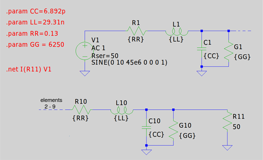
3.1 Spice simulation
Because the CUT is a sample of 1.0 m in length and the maximum frequency is 500 MHz in the case of the S-parameter measurement, the simulation model has been split into pieces of 0.1 m for the purpose of the simulation. The PUL data acquired are divided by 10 as far as L′ and R′ are concerned, C′ and G′ are multiplied by 10. In total, the CUT in the simulation represents 1.0 m, and the condition of segments being significantly shorter than λ/10 is still satisfied.
The model in Figure 1 shows 10 sections, each of them with 4 lumped elements (R1, L1, C1, G1 to R10, L10, G10, C10), the termination of the model represented by R11 and the respective parameters which are applied to all elements. To get S-parameters from the schematic, the directive .net I(R11) V1 is used. This parameter set provides the result given in section 4 in Figure 6.
3.2 Finite element method
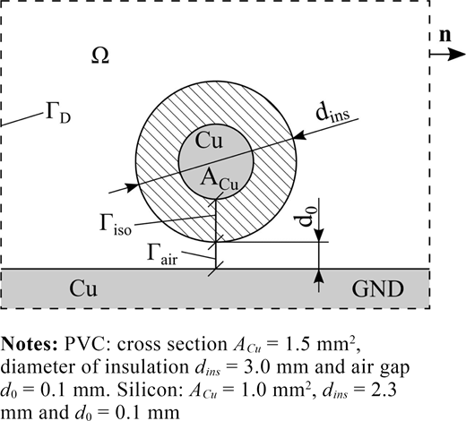
The benchmark with details is presented in Figure 2 and consists of a PVC or silicon insulated copper wire above a copper plate. The length of the wire has been selected to be 1.0 m, and the copper plate with a thickness of 0.5 mm is assumed to have infinite dimensions. The air gap represents an estimated average in contrast to the physical setup of the measurements.
The basic boundary value problem to be solved in the frequency domain reads
where A is the magnetic vector potential (MVP), μ the magnetic permeability, σ the electric conductivity, ε the electric permittivity, j the imaginary unit, ω the angular frequency, some Dirichlet boundary condition, Ω the problem domain, ΓD the Dirichlet boundary and n the unit normal vector, see Figure 2. The domain Ω comprises air, copper wire, insulation and GND, respectively, where ΓD is its outer boundary. The following considerations for the FE simulations are based on a Cartesian coordinate system. The transversal fields are lying in the drawing plane, compare with Figure 2. The direction of propagation corresponds to the z-coordinate. The problem for the FE simulations is assumed to be infinitely long in the direction of propagation. To take into account the specific nature of the present problem, the MVP has been decomposed into two components, a transversal component lying in the drawing plane and Az(x, y), which points into the direction of propagation
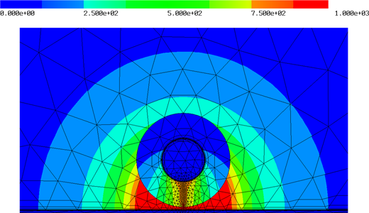
where with and for the FE approximation indicated by the additional index h, see Schöberl and Zaglmayr(2005). Because the dependence of A in equation (5) with respect to z is known, a two-dimensional FE model suffices. The lumped elements R′, C′, etc., have been calculated based on the corresponding losses and energies PUL in the electromagnetic field. For instance, C′ has been determined with the electric energy due to the transverse electric field , which is shown in Figure 7, and R′ with the aid of the losses caused by currents due to the electric field component . The lumped elements are obtained by
respectively. The voltage U between the copper wire and ground plate is prescribed to excite the problem; the current I is obtained by means of simulation. The z-components of the current densities in the wire and in the ground plate are opposed. The current in the copper wire should theoretically match the current in the GND plane except for the sign. The cross-sections of the copper wire and of the GND-plane are completely different; consequently, their FE-meshes too. Therefore, one cannot expect an exact match of the two currents because of numerical inaccuracies. For instance, prescribing U = 1 V yields, I = –0.01411 – j0.00013 A in the wire and I = 0.01461 + j0.00061 A in the GND-plane, which is satisfactorily accurate.
Transverse electric field for the PVC insulated wire, detail. The FE model consists of 13,160 elements
Transverse electric field for the PVC insulated wire, detail. The FE model consists of 13,160 elements
4. Results
All data shown were acquired with CUTs 1.0 m in length or referred to as 1.0 m as far as simulation data are concerned.
4.1 Frequency domain data
The measurement in the frequency domain was performed using a 2-port VNA (ZVL6). Both ends of the CUT are connected to the VNA, which represents a termination with 50 Ω at either end. The obtained set of S-parameters was subsequently converted into RLGC-data. The results with the given PVC-insulated conductor can be seen in Table 1.
Frequency domain, PVC
| Parameter | PVC black | PVC red | Unit |
|---|---|---|---|
| f | 59.46036 | 57.46873 | MHz |
| Zl | 65.21131 | 63.88990 | Ω |
| R | 1.325222 | 4.935247 | Ω |
| L | 293.0912 | 285.8608 | nH |
| C | 68.92185 | 70.03098 | pF |
| G | 1068.469 | 704.8839 | μS |
| vp | 2.224949 · 108 | 2.235000 · 108 | m/s |
| vf | 0.7416498 | 0.7450001 | 1 |
| td | 4.494484 | 4.474273 | ns |
| εr,eff | 1.818035 | 1.801720 | 1 |
Measurements of a red and black silicone-insulated conductor show a similar picture, and the obtained results are given in Table 2.
Frequency domain, silicone
| Parameter | Silicone black | Silicone red | Unit |
|---|---|---|---|
| f | 59.33388 | 55.78086 | MHz |
| Zl | 70.32518 | 69.65358 | Ω |
| R | 2.415429 | 1.786379 | Ω |
| L | 307.7858 | 305.5429 | nH |
| C | 62.23388 | 62.97747 | pF |
| G | 639.8732 | 284.2796 | μS |
| vp | 2.284874 · 108 | 2.279667 · 108 | m/s |
| vf | 0.7616247 | 0.7598888 | 1 |
| td | 4.376609 | 4.386607 | ns |
| εr,eff | 1.723923 | 1.731809 | 1 |
It is important to note that the conductors with different colored insulators exhibit differing RLGC parameters. This will also be addressed in Section 4.2.
The data extraction requires some arithmetic: The test point chosen is the lowest frequency minimum of the imaginary part of ZS11, the impedance of the CUT derived from S11, as can be seen in Figure 3 for the conductor with the black PVC insulator.
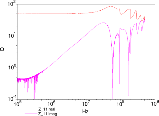
The impedance seen at Port 1 of the VNA equals
and considers the magnitude and phase of the real and imaginary parts of ZS11.
4.2 Time domain data
As mentioned above, the TDR test set is used to acquire the “flight time” of a pulse incident on the CUT. The effective permittivity εr,eff can directly be derived from the time delay as given by the TDR test set using
with vf being the velocity factor of the wave on the CUT, which is always ≤1, and
with c0 being the speed of light in a vacuum and l being the length of the CUT.
Tables 3 and 4 show the parameter “unit” which has not been explained so far. TDR measurements usually normalize the amplitude of the reflected wave to the system impedance. A full reflection from an open terminated cable is then represented by a unit of 2, whereas no reflection at the end of a cable, i.e. a proper termination with the impedance of the conductor, will show a unit of 1.
Time domain, PVC
| Parameter | PVC black | PVC red | Unit |
|---|---|---|---|
| Flight time | 9.732 | 9.568 | ns |
| td | 4.866 | 4.784 | ns |
| vf | 0.6855 | 0.6973 | 1 |
| εr,eff | 2.128 | 2.057 | 1 |
| rf | 0.145 | 0.136 | 1 |
| Zl | 66.95 | 65.74 | Ω |
| Parameter | PVC black | PVC red | Unit |
|---|---|---|---|
| Flight time | 9.732 | 9.568 | ns |
| td | 4.866 | 4.784 | ns |
| vf | 0.6855 | 0.6973 | 1 |
| εr,eff | 2.128 | 2.057 | 1 |
| rf | 0.145 | 0.136 | 1 |
| Zl | 66.95 | 65.74 | Ω |
Time domain, silicone
| Parameter | Silicone black | Silicone red | Unit |
|---|---|---|---|
| Flight time | 9.78 | 9.624 | ns |
| td | 4.89 | 4.812 | ns |
| vf | 0.6821 | 0.6927 | 1 |
| εr,eff | 2.149 | 2.0839 | 1 |
| rf | 0.189 | 0.187 | 1 |
| Zl | 73.30 | 73.00 | Ω |
| Parameter | Silicone black | Silicone red | Unit |
|---|---|---|---|
| Flight time | 9.78 | 9.624 | ns |
| td | 4.89 | 4.812 | ns |
| vf | 0.6821 | 0.6927 | 1 |
| εr,eff | 2.149 | 2.0839 | 1 |
| rf | 0.189 | 0.187 | 1 |
| Zl | 73.30 | 73.00 | Ω |
A fraction or a multiple of a unit is consequently a measure of the impedance of the cable, as outlined in Figure 4.
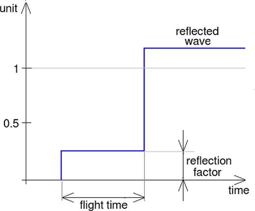
The “flight time” mentioned earlier is the time a pulse incident into the CUT takes until it returns from the open end of the CUT. The pulse “travels” two times the cable length; therefore, the delay time td is half the “flight time”. The “reflection factor” mentioned in Figure 4 can be converted into an impedance value of the CUT by means of the following equation
where Zl represents the characteristic impedance of the CUT and rf the reflection factor with a sign.
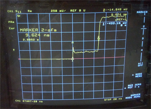
A representative measurement is shown in Figure 5.
4.3 Spice results
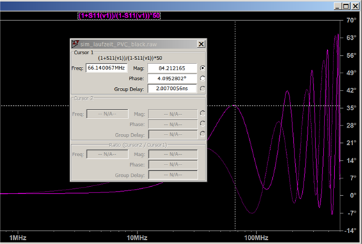
To verify the applicability of the model data and their match to measured results, the acquired cable data of “PVC black” have been used. It is clear that the idealized simulation because no parasitics are considered, shows minor deviations. Yet, a first verification with the resonant frequency shows a satisfying match, as given in Figure 6.
The trace shows ZS11 derived from S11 using equation (7) but a blank and the resonance at 66.14 MHz, which is a close match to the measurement results.
4.4 Finite element simulations
Homogenous Dirichlet boundary conditions and Az = 0 are selected on ΓD. The shortest line from the copper wire to GND consists of Γiso and Γair, compared with Figure 2. A voltage of U = 1 V as excitation is prescribed by the tangential component of along Γiso and Γair corresponding to ϵr of air and insulator and the lengths of Γiso and Γair, respectively.
Simulations have been carried out with Netgen/NGSolve (Schöberl, 2021). The transversal electric field is obtained by
a field plot is presented in Figure 7. The measurement and simulation results are summarized in Table 5. No losses have been considered in the insulation; G′ solely takes into account losses due to the transverse field in copper, which explains the large difference between measurement and simulation. The true values of several parameters are not known. To study the influence on transmission line parameters (TLPs), several simulations have been carried out. The uncertain parameters have been varied in a meaningful and feasible range. Results are presented in Tables 6–8. The influence of εr on the TLPs is big, whereas that of d0 and dins is rather moderate. However, it is worth mention that for a very small d0 and a feasible FE mesh, the limit value C′ = 93.5 pF has been found.
Measurement and simulation results
| Measurement | Simulation | ||||
|---|---|---|---|---|---|
| Parameter | Unit | PVC | Silicone | PVC | Silicone |
| f | MHz | 59.3 | 59.5 | 59.3 | 59.5 |
| R′ | Ω/m | 1.33 | 2.42 | 1.19 | 1.45 |
| L′ | nH/m | 293 | 308 | 306 | 293 |
| C′ | pF/m | 68.9 | 62.2 | 81.8 | 72.9 |
| G′ | mS/m | 1.07 | 0.64 | 0.12 | 0.14 |
| Zl | Ω | 65.2 | 70.3 | 61.1 | 63.4 |
Relative permittivity of the insulator
| εr | R′ | L′ | C′ | G′ | Zl |
|---|---|---|---|---|---|
| 1 | Ω | nH/m | pF/m | mS/m | Ω |
| 3 | 1.15 | 302 | 71.0 | 0.11 | 65.2 |
| 4 | 1.19 | 306 | 81.8 | 0.12 | 61.1 |
| 5 | 1.22 | 309 | 90.5 | 0.12 | 58.4 |
| εr | R′ | L′ | C′ | G′ | Zl |
|---|---|---|---|---|---|
| 1 | Ω | nH/m | pF/m | mS/m | Ω |
| 3 | 1.15 | 302 | 71.0 | 0.11 | 65.2 |
| 4 | 1.19 | 306 | 81.8 | 0.12 | 61.1 |
| 5 | 1.22 | 309 | 90.5 | 0.12 | 58.4 |
5. Conclusions
Measurements in the frequency domain and in the time domain show a reasonably accurate match of the results.
It needs to be said that both approaches complement and confirm each other. The FD testing requires a terminated line (with the system impedance), the TD testing needs an open line end, i.e. without termination matching the system impedance.
Future work will extend the model to extract estimated emissions from a single conductor as well as bus structures at frequencies of interest. This will be examined with and without a grounded plane with subsequent verification and matching to get reliable simulation models. Three-dimensional FE models will be used to appropriately simulate relevant emissions. The simulation models shall be optimized for fast and reliable simulations based on a sensitivity analysis showing the impact of parameter variations like d0 in Figure 2.
