
JPCA. Japan Printed Circuit Association
JPCA (Japan Printed Circuit Association)
Keywords Japan, JPCA, Printed circuit boards
Introduction
JPCA is the abbreviation for Japan Printed Circuit Association, and was established in 1962 as a voluntary organization. In 1977, JPCA became the only printed circuit industry organization in Japan to be approved by the Ministry of International Trade and Industry (MITI). The organizational structure of the JPCA is given in Figure 1.
JPCA aims to improve both quality and performance of printed circuit industry and related industries. Thereby, it play a major role in promoting the progress and development of electronics technology and improving performance of electronic equipment with the objective of contributing to overall economic development.
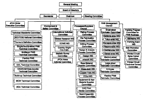
Figure 1The organization structure of JPCA
JPCA's current membership is made up of 503 corporations. Breakdown in terms of categories is as follows:
Fifty per cent printed wiring boards/printed circuit boards manufacturers,including sectional processers for PWBs/PCBs fabrication.
Twenty-five per cent corporations engaged in manufacturing and sales of machinery or equipment for PWBs/PCBs fabrication.
Twenty-five per cent corporations engaged in manufacturing and sales of base materials or related material for PWBs/PCBs fabrication.
Some types of projects involved include the following items:
Management improvement of printed circuit board manufacturing business classified by company size or area.
Hosting JPCA shows.
Hosting international symposia/seminars or meetings.
Drafting Japan Industrial Standard (JIS).
Deliberations on International Electrotechnical Commission (IEC) Standard.
Survey on technological and demand trends.
Holding various committees, sub-committees relating to corporate management.
Publication of periodical journals, such as JPCA News.
Collaboration on conducting the national proficiency test for PWB/PCB technology, including design, fabrication.
Conducting the national proficiency test for commercial skill of printed wiring board business and raising the printed circuit sales careers.
Environment and safety standardization.
Collaboration and co-operation with relative industrial associations,academic societies, national/international institutions.
Sponsoring Electronic Circuits World Conventions (ECWCs).
Printed wiring boards output transition in Japan
Year by year output transition of printed wiring board in ten years, starting from 1988, is shown in Table I and Figure 2.
 Table I
JPCA's Statistical Research Project has been annually conducted since 1968. The programme is one of the most important services at JPCA, and it will be continued in the future.
The rapid increase for build-up PWBs, BGA/CSP substrates for IC package is remarkable, as shown in Table II and Figure 3. JPCA must be sensitive to market movements.
The National Proficiency Test for PWB/PCB technology
The strength of the PCB industry lies in the fact that its substantial ability is cultivated by employees with high skill levels who are developing new technology. The JPCA has been conducting the National Proficiency Test for PWB/PCB technology,collaborating with the Ministry of Labor since 1989. The certificate examinations are graded 1, 2, 3, with the highest level indicating the degree of difficulty. Each test graded 1, 2, and 3 is classified by both design work and fabrication, and includes a theory examination and practice. A successful applicant in both examinations can obtain the certification approved by the Ministry of Labor, and he/she can achieve important positions in firms. Year by year the examinees and passers progress through the examinations as shown in Tables III and IV. In order to succeed in the examinations, the examinees must be well-informed in PWB/PCB technology such as terms and definition, design,manufacturing methods, quality control, environmental safeguard, laws, and possess well-honed skills.
 Figure 2 Output transition classified by product type
 Table II
The JPCA have also conducted the National Proficiency Test for Commercial Skills of PWB Business since 1996, in order to raise business sense and ability. The JPCA thereby promoting the improvement of both technology and business quality in the whole industry through these training programmes.
As the JPCA described in the Report on the Strategy for the Electronic Circuits Industry, the targeted future PCB industry could not acquire all the technological resources it needs through development alone. It also needs to be equipped with well-honed skills and know-how. The Japanese word for well-honed skills is takumi. The meaning is supposed to be close to that of the word craftsmanship. Takumi,or craftsmanship, is precisely what is needed for evolution into the electronic circuits industry (Figure 4).
Standardization
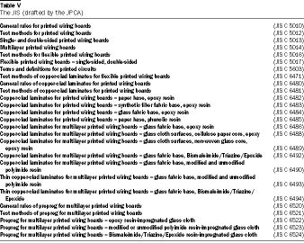
The JPCA has been drafting the JIS on Printed Circuit Technology and conducting deliberations on International Electrotechnical Commission (IEC)/TC52 Standard since 1983 (Table V). The JIS acts on the same lines as IEC and has recently introduced a new quality assessment system, so that the publication series of the JIS could be radically revised. The JPCA drafting of the JIS will re-examine all the standards related to IEC/TC52.
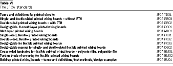
The JPCA will also agree a new joint standard such as build-up printed wiring boards with new fabrication processes and a quality guaranteed basis for flexible printed circuit boards, in co-operation with the IPC (Table VI).
In order to establish a global standard of PCB, the JPCA believes that many PCB trade associations should be involved in the standardization activity and increase the collaboration between the world federations than previously.
International liaison activities
ECWCs (formerly PCWCs) are to be held every three years, rotating between three economic block areas,Europe, the Americas and Asia. After changing the name of the World Convention,the Policy Committee, which is formed by four sponsoring organizations, EIPC,IPC, UK Committee (PCIF and IMF), and the JPCA, widened the category of suggested topics, according to the changes in the time and the industrial structure. ECWCs will be a forum where various industries can meet together and exchange a new technological and management information on an international basis.
ECWCs will lead in this initiative and announce the information, such as advanced technologies,grappling with environmental difficulties, new management methods, etc., to all the related industries.
Although ECWCs are hosted by joint sponsorship of the four international associations, a venue at which all the associations could be seated to discuss the common issues had not previously existed. As a trial of holding an international associations meeting,the JPCA offered an opportunity for delegates, including EIPC, IPC, PCIF, who attended the ECWC Policy Committee in June, to meet and share information on global industry trends. At the previous meeting, timed to coincide with the JPCA Show '98, the two Asian trade associations, CPCA of China and TPCA of Taiwan,whose aims are to promote the industry development, also participated.
 Figure 3 Output transition of particular PWBs classified by product type
 Table III
 Table IV
Increasing globalization will continue and major challenges facing the industry, such as customer satisfaction, materials procurement, investment in plant and equipment, and personnel education, will become increasingly international. Only through continued and expanding co-operation between the industry associations can these global challenges be successfully addressed.
In future, the conventional industrial structure, of which bare board fabrication was the center, will include not only an industrial segment for interconnection and packaging, but will also border the semiconductor industry. Expanding the industrial boundaries and cultivation of new domains will create a new market.
Only ECWC sponsoring organizations cannot develop all the information. This can be most effectively and efficiently accomplished through co-operation and productive liaisons between industry associations, maintaining contact with other associations in the same region, Europe, the Americas, and Asia. Co-operation on other issues that affect our industry are best addressed through co-operation among the trade associations internationally.
International co-operation is not confined to only holding ECWCs, co-operation will advance a new shape for international formation of the industry associations to overcome strategic problems.
JPCA show/international associations meetings
There are four major PCB industrial trade-shows world-wide, the CPCA Show in Shanghai, China, IPC Expo in the USA, the JPCA Show in Japan and the new EFIP Show "EPC Convention" in Europe. Most important, all four of these trade-shows are owned by the industry. We are all managed by trade associations and any profit we make is reinvested in the industry resulting in better political activity, more technical support and better commercial information. The work undertaken by these growing trade associations clearly benefits the whole industry.
Another useful outcome of trade association involvement is that all these exhibitions bring with them conference or symposium programmes of international standing. All four offer an extensive list of papers that give the delegate a chance to be informed and educated while having sufficient time to visit the show. The trade associations or academic societies take very seriously the selection of papers for such events and are justifiably proud of the reputation we have for holding informative and interesting events. The organization of such conferences is complex and a large effort is needed to provide the right venue, structure and support for these presentations.
These conferences provide another important function in that they offer an opportunity for delegates from around the world to meet and share information on global markets and technologies. The industry associations are responding to this opportunity through the establishment of a series of international association meetings timed to coincide with the trade shows. Following a preliminary meeting in January 1997, the JPCA hosted the first international association meeting, as a trial in Tokyo, in June 1998. Representatives from the JPCA, IPC, EFIP (EIPC and PCIF), CPCA, and TPCA attended. Chaired by Masaru Endoh, JPCA chairman (Ibiden),the meeting reflected his open and energetic style. Discussion focused on issues of common concern to the international interconnection and packaging community,including capacity expansion, quality, training, and the environment. It was generally felt that we needed to work more closely together for the good of the industry, and the EFIP hosted the meeting at the EPC Show, at Wiesbaden, in September 1998.
The JPCA show, held annually in June, is recognized throughout the world an ideal meeting place,where all the technologies relevant to printed circuitry are assembled and exhibited. As a trade show for a single industry, it is considered a world leader in its field.
Printed circuitry is produced by many varied processes, and is a product that enables the futuristic potential of electronics technologies to be exploited. As such, it constantly faces the challenges of pursuing and excelling in the creativity and reliability, of its technology, not only for the printed circuitry, but for its materials, its manufacturing facilities and test apparatus.
JPCA believes sincerely that our JPCA show, which exhibits the results of the constant endeavors all the people in the industry, will contribute to the further progress and business success of not only the printed circuit industry, but also the entire electronic circuits industry. The JPCA show is a trade show, which the printed circuit industry originated and has continually promoted. In addition to the exhibits,we trust all participants will find it to be an excellent forum to exchange information and to develop business opportunities. The JPCA have been hosting the JPCA Show with a consistent policy for 27 years, may it long continue.
About JPCA Show '99
Date: Wednesday, 2 June-Friday, 4 June 4 1999, three days.
Location: Tokyo Big Sight(21-1, Ariake 3-chome, Koto-ku, Tokyo 135-0042, Japan).
 Figure 4 (a) Definition of the electronics circuit industry: well-honed skills and know-how; (b) The Japanese for takumi (craftsmanship)
Required qualification:producers of printed circuits and electronic packages thereof, producers of relevant materials, machinery and equipment, producers of materials, machinery and equipment for the recycling and other environment protection activities related to the above, trading companies and associations related to the above,all regardless of location and nationality.
Period for exhibitors'applications: 1 October 1998-5 February 5 1999.
Special research activities of the JPCA, 1982-1998
The JPCA has conducted special research activities, such as settlement of the industry vision,technology road-map for promoting and improving the PCB industry in Japan since 1983. The titles issued previously include:
Report on the Long-range Vision for PWB Industry, issued in 1982.
Report on the Trend Survey of New PWB Technology, issued in 1983.
Report on the Trend Survey of Multilayer PWB, issued in 1984.
Report on the Trend Survey of New Assembly System for PWB, issued in 1985.
Report on the Trend Survey of Ceramic PWB, issued in 1986.
Report on the Strategy for the Printed Circuit Industry, issued in 1987.
Report on the Trend Survey of Surface Mount Technology, issued in 1988.
Report on the Trend Survey of PCB Design and Fabrication System,issued in 1989.
Report on the Trend Survey of PCB Technology in EMI/EMC, issued in 1991.
Report on the Trend Survey of New Surface Mount Technology, issued in 1992.
Report on the Long-range Vision for PCB Industry, issued in 1993
Report on the Strategy for the Electronic Circuits Industry, issued in 1996.
This year JPCA issued Report on the Technology Road Map for Advanced System Integration and Packaging,according to the special research activities. The purpose and brief contents are as follows.
The purpose
We have seen the full-scale advent of the multi-media age and the progress of new informationoriented society, which have been brought about by the rapid spread of personal computers, fast development of world-wide networks typified by Internet and intranets, and the construction and expansion of a mobile data communication infrastructure by digital cellular phones and the Personal Handy-phone System (PHS). Accordingly, the leadership of the information society has been increasingly transferred to individuals. Because of this, development of new electronic hardware equipment, which enables us to send and receive easily the real time information such as image, voice and video anywhere, is desired earnestly.
Further technical development in many fields and the integration of these technologies are indispensable for achieving such devices. From the viewpoint of the electronic packaging technology, however, the establishment of "the advanced system integration and packaging technology" such as "how to refine the high-performance and high-function circuits into small, lightweight and high-speed circuit modules within three or five years at low cost" is required for the basic technology of development and realization of electronic hardware equipment.
In short, there may be a common understanding that the establishment of "the next-generation high-speed micro-circuit electronic packaging technology" is the key for the development of small-size, lightweight, high-function and integrated electronic devices, which are excellent for personal use. Persons concerned request that it is necessary to carry out comprehensive research and study on such matters as "how further will this technology advance?" or "by which needs will new progress be accelerated?"
So, in order to obtain the technical guideline by clarifying the actual state of current electronic packaging technology and identifying both the possibility of development and the prospect of the next-generation technology, "trend research of the advanced system integration and packaging technology packaging technology" was carried out and the report of this research was published. The purpose of this research was to contribute to the sound progress of the electronics industry through the activities mentioned above.
Inauguration of the Study Committee on the Technology Road Map for Advanced System Integration and Packaging
In order to accomplish the purpose of the research shown above, the Study Committee on the Technology Road Map for Advance System Integration and Packaging, consisting of 19 members,representing manufacturers of electronics equipment, semiconductors, electronic components, printed circuit boards, facilities and materials, as well as academics and experienced people, was inaugurated in May 1997. Through the six main committee meetings, the following subjects were discussed (the committee members are shown in the next section).
Main subjects discussed:
- 1.
Discussions about the method of research.
- 2.
Preparation of the questionnaire.
- 3.
Discussions about collection and summarization of the questionnaires.
- 4.
Analysis of the summarized data.
- 5.
Preparation of the draft of the report concerning Technology Road Map for Advanced System Integration and Packaging and discussion about the contents of this report.
Outline of the research activities
As the result of discussion in committee, it was determined to conduct the research by this working group, mainly in the trends of the following four matters with set manufactures as the subject of the research:
- 1.
electronic hardware equipment;
- 2.
semiconductor devices and electronic components to be mounted;
- 3.
change of IC package shape; and
- 4.
interconnection and packaging technology.
The responses were collected according to the following procedures.
1. Research items:
- 1.
Trends of the next generation electronic hardware equipment.
- 2.
Trends of the next generation ICs and LSI Packages.
- 3.
Trends of the next generation of SMDs and electronic components.
- 4.
Trends of material characteristics of the next generation IC substrates/PWBs.
- 5.
Trends of the next generation substrates and PWBs.
- 6.
Trends of the next generation interconnection and packaging technology.
- 7.
Trends of the next generation test and inspection technology.
- 8.
Trends of the next generation tools for design/analysis-support and manufacturing system.
2. The subject products of this research:
- 1.
Mobile PC.
- 2.
PC card.
- 3.
Mobile communication tools (cellular phone).
- 4.
Mobile communication tools (personal handy phone system (PHS)).
- 5.
Wireless paging device (pager, etc.).
- 6.
Personal digital assistant (PDA).
- 7.
IC card.
- 8.
Camcorder with LCD monitor (VCR).
- 9.
Digital still camera.
- 10.
DVD player/recorder.
- 11.
Navigation system.
- 12.
Composite electronic equipment.
3. Term for response to the survey: from 12 September 1997 to 17 October 1997.
4. Actual results of sending and collection of questionnaires:
The questionnaires were sent to 88 divisions of 44 set manufacturers (171 questionnaires in total) in Japan, from which 74 questionnaires have been collected (collection rate: 43.2 per cent).
Main contents of the report
Chapter 1: Introduction. Chapter 2: Trends of the Next Generation Electronic Hardware Equipment. Chapter 3: Trends of the Next Generation ICs and LSI Packages. Chapter 4: Trends of the Next Generation SMDs and Electronic Components. Chapter 5: Trends of Material Characteristics of the Next Generation IC Substrates/PWBs. Chapter 6: Trends of the Next Generation Substrates and PWBs. Chapter 7: Trends of the Next Generation Interconnection and Packaging Technology. Chapter 8: Trends of the Next Generation Test and Inspection Technology. Chapter 9: Trends of the Next Generation Tools for Design/Analysis-Support and Manufacturing System. Chapter 10: Business Outlook for Advanced System Integration and Packaging Technology. Chapter 11: Current Progress in Optical Interconnections and their Impact on the NextGeneration Packaging Technology.
This comprehensive report discusses the next generation technology trends and the market of PCB industry as well as plans for the establishment of a new electronic circuits industry!The issues and challenges faced by all PCB manufacturers and the new directions they are exploring will be of interest to anyone who manufactures, assembles or uses advanced PWBs/IC substrates and PCB industry suppliers. (321 pages, in Japanese); a version in English will be available at the IPC soon.
Sister organization
There was another organization related to PCB industry in Japan, namely Japan Institute for Interconnecting and Packaging Electronic Circuits (JIPC), which was established in April 1986, as an academy supported by JPCA. It aims to promote education, R&D,technology and initiate approaches to major technical issues through co-operation among industry, government and academia on interconnecting and packaging electronic circuits.
In Japan SHM, that started as ISHM (IMAPS) Japan existed, and it aims were specifically to promote hybrid microelectronics and packaging technology to the industry. The two academic societies of JIPC and Society for Hybrid Microelectronics (SHM), as an independent organization, were conducting respective activities. However, change in industrial structure, the breaking down of technological borders and new technology innovations removed a fence between two academic societies related to electronic packaging in Japan.
A new organization, the Japan Institute of Electronics Packaging was launched on 1 April 1998, in order to integrate two key technologies, namely microelectronics and packaging. The JIPC and the SHM merged to form this new Institute. JIEP will serve as a base for even higher and wider development and success of the entire PCB/interconnection and packaging related industry.
Conclusion
JPCA is a unique organization because of the constituent members, PWB/PCB fabricators,set-manufactures of electronic equipment, sectional processers, base material suppliers, suppliers of raw material, machinery or equipment. Industrial development depends on the strong links between different enterprises from the viewpoint of printed circuit technology development, quality advancement,commercial custom improvement, rationalization of distribution sector in the PCB industry. Relationships between the different companies are promoting and raising a healthy industry.
JPCA has strived to achieve the goal of promoting and toughening the domestic industry. However,JPCA is now responsible for providing the Asian region with guidelines for the development of the Asian PCB industry in the twenty-first century, as well as to contributing to the further development of the global industry. JPCA intends to promote further information-sharing with other international PCB trade associations in order to improve the status of the world-wide PCB industry.
JPCA headquarters office
There are other three organizations related to JPCA at JPCA headquarters office, KAIRO, KAIKAN, Japan Institute of Electronics Packaging (JIEP) of the academic society on the first floor, Japan Printed Circuit Health Insurance Association on the third floor,and Japan Printed Circuit Welfare Annuity, found on the fourth floor.
Japan Printed Circuit Association, Kairo Kaikan 2F, 12-2, Nishiogikita 3-chome, Suginami-ku, Tokyo 167-0042 JAPAN. Tel: +81-3-5310-2020; Fax: +81-3-5310-2021; e-mail: jpca9@jpcanet.or.jp URL: http://www.jpcanet.or.jp


