

The purpose of this paper is to present the properties of thick-film resistors made of novel pastes prepared from glass and graphite.
Graphite-based resistors were made of thick-film pastes with different graphite-to-glass mass fraction were prepared and examined. Sheet resistance, temperature coefficient of resistance, impact of humidity and short-term overload were investigated. The properties of the layers fired in atmospheres of air at 550°C and nitrogen at 875°C were compared.
Graphite-based resistors with various graphite-to-glass ratios made possible to obtain a wide range of sheet resistance from single O/square to few kO/square. These values were dependent on firing atmosphere, paste composition and the number of screen-printed layers. The samples made of paste with 1:1 graphite-to-glass ratio exhibited the temperature coefficient of resistance of about −1,000 ppm/°C, almost independently on the firing atmosphere and presence of a top coating. The resistors fired in the air after coating with overglaze, exhibited significantly lower sheet resistance, reduced impact of humidity and improved power capabilities.
In this paper, graphite-based resistors for applications in typical high-temperature cermet thick-film circuits were presented, whereas typical graphite-based resistors were fabricated in polymer thick-film technology. Owing to very low cost of the graphite, the material is suitable for low-power passive circuits, where components are not subjected into high temperature, above the typical temperature of operation of standard electronic components.
1. Introduction
Carbon-based composite materials with proper fillers could exhibit temperature of operation up to 700°C. Therefore, they are useful in electronics, where harsh conditions are present, e.g. during an electrical discharge or an electron emission. So far, various carbon-based composites were reported to work as transparent conductors (Watcharotone et al., 2007), resistive layers (Dziedzic, 1997, 2005; Rao, 2007; Mleczko et al., 2017) or as an active part in sensors for detection of chromium (Hallam et al., 2010), proteins (Gómez-Mingot et al., 2011) or heavy metals (Aragay, Pons and Merkoi, 2011). However, in the literature, it is not clearly defined what are the electrical properties of the graphite and graphene layers/paths. For example, Marinho et al. (2012) used the same technology to prepare the layers from graphene, graphite and carbon black. It shows that the conductivity of the graphene layer is one order of magnitude higher than graphite and on only twice higher than carbon black. The authors claim the reason was lying in a wide spectrum of techniques to deposit a layer. Besides, various components were used to form composites, i.e. solvents and additives including fillers. For example, the glass filler can reduce the conductivity, but at the same time, it can increase layer reliability, especially at high temperature (> 300°C). In contrast, the layers with another filler material, such as polymers, are stable up to 300°C.
Graphite is a crystalline allotropic form of carbon with a hexagonal structure. This material is very common in the world, from the simplest applications such as pencils to more advanced ones such as control rods in nuclear reactors. Electrical parameters of that material allow to use it in a production of electronics, e.g. in a form of conductive inks or resistive layers in a form of a polymer thick-films. For the last purpose, typical materials used for resistive layers are IrO and RuO2 in a glass matrix (Pike and Seager, 1977). These materials present very good electrical stability and repeatability. However, comparing to polymer layers, cermet materials are much more expensive.
Graphite and carbon-black are widely used as a conductive phase in a polymer thick-film resistive layers made with various matrix materials as PVC and PMMA (Murthy et al., 1984; Zheng and Wong, 2003). The works cover the experiments on laser trimming of resistance, examination on resistance change in the function of humidity and temperature (temperature coefficient of resistance [TCR]) and impact of high voltage pulse on the resistance change. Also, new nanomaterials as graphene and carbon nanotubes were popular in printed electronics from their appearance, but generally in high conductivity layers, e.g. for using as detecting electrodes Hallam et al. (2010), Gómez-Mingot et al. (2011), Aragay et al. (2011). Polymer films do not require special ovens, because its curing temperature is below 300°C. Curing temperature has a big influence on their electrical parameters. The reduction of the process temperature down to 150°C can reduce costs but can also deteriorate the parameters. Besides, thanks to the lower temperature, the polymer layers based on carbon-black and graphite can be applied on flexible or FR4 substrates.
Generally, typical thick-film pastes are based on particles of a conductive material, an organic vehicle and a glass as a bonding medium (White, 2017). The organic vehicle is very important for the process of screen printing, because it gives proper viscosity. Weight content of the glass in pre-fabricated pastes should be checked experimentally. Percolation edge calculation could be not enough to fabricate such pastes. Besides, the organic vehicle ensures initial adhesion of grains to the substrate. Glass used in the paste mixture has significant influence on technology, cause after curing and reflow process of the glass, that material makes adhesion of conductive grains to the substrate. Adhesion also depends on the ratio of the functional material to the glass in the composite.
In case of this study, we focussed on thick-film pastes with graphite grains as a functional material and a glass as a bonding medium. The authors developed and fabricated novel material in a form or graphite–glass composite for application as screen-printed resistive layers. The material takes the advantages of both types of thick-film resistor pastes – cermet and polymer. Low cost of the graphite, extended temperature of operation limited mainly by oxidation of graphite and possible application in standard thick-film circuits make the materials competitive to typical thick-film resistor material for standard applications.
2. Materials and methods
During the experiment, three various pastes were fabricated with 3:1 mass ratio glass/graphite (P1), 1:1 mass ratio glass/graphite (P2) and 1:3 glass/graphite (P3) mass ratio. Synthetic graphite (Sigma Aldrich) with mean grains below 20 µm was used. Pastes were fabricated from glass (SG-683K, Heraeus) and acrylic vehicle. In the experiment, we used ceramic substrates Al2O3 96% with screen-printed PdAg electrodes (7484 R, Du Pont). Electrodes were fired at a peak temperature of 875°C. Design of the resistors geometry is presented in Figure 1, and their geometrical parameters are presented in Table 1. For the graphite pastes, the deposition process was performed using 200-mesh stainless steel screen with 30-µm emulsion.
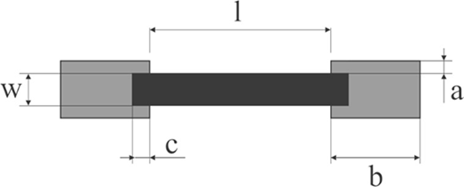
Geometrical parameters of resistors
| Parameter | Description | Value |
|---|---|---|
| l | Resistor length | 2; 3; 4; 5; 6; 7; 8; 9; 10 mm |
| w | Resitor width | 1 mm |
| a | Extension of termination width | 0.25 mm |
| b | Termination length | 2 mm |
| c | Termination overlap | 0.5 mm |
Preliminary experiments showed that value b should be greater than 0.25 mm because the contact resistance is determined by not only contact area but also density of conductive grains, the most significant for of paste P1. Also, a porosity of printed layers determined a minimum number of layers. In the experiment, minimum two layers were printed. For examination of a sheet resistance of each paste, 2, 3 or 4 layers were screen-printed. Various firing temperatures were used, dependently on the atmosphere in the oven. The technology course of the samples is presented in Figure 2.
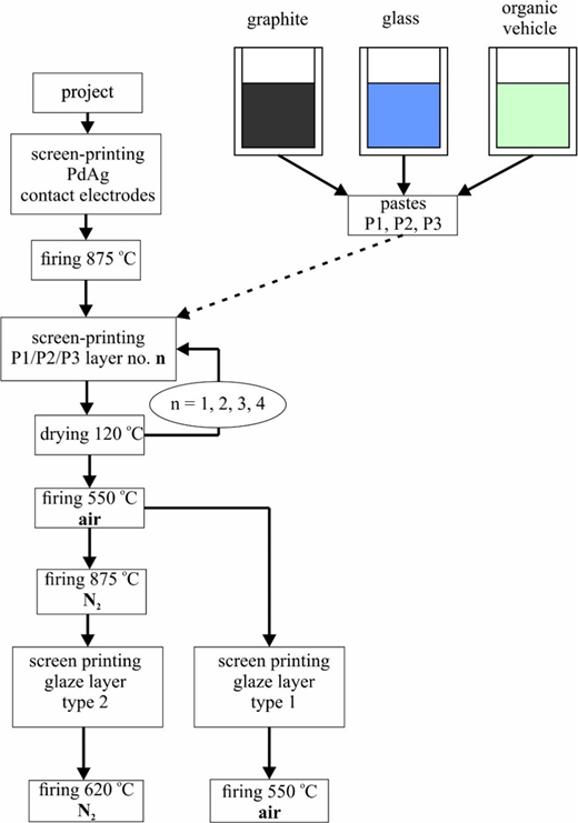
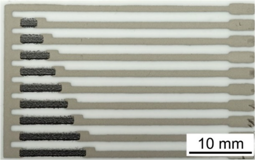
The samples consisted of resistors with nine different lengths, as listed in Table 1. Influence of length on the sheet resistance was important for compatibility testing of the contact material and resistive layer because it was possible to observe a contribution of contact resistance to total resistance of the component. The samples were arranged on the substrate as shown in Figure 3. Such placement made possible to use edge connectors to multiplexed measurement unit and simultaneous testing of a whole series of the components.
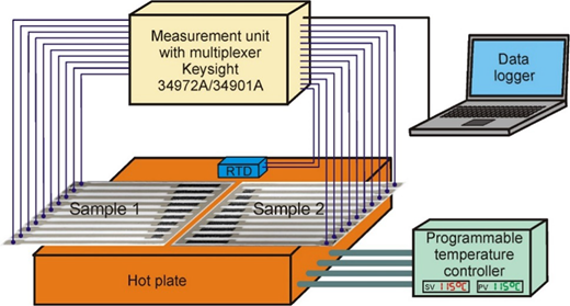
Test setup shown in Figure 4 was used during measurement of sheet resistance, TCR and impact of humidity for the series of test samples. The setup consisted of a programmable measurement unit with 20-channel multiplexer (34,972 A with 34,901 A card, Keysight). During TCR determination, the samples were placed on a hotplate with programmable temperature ramp. The data were logged on a PC.
3. Results
3.1 Sheet resistance measurements
The resistance of test samples was determined at room temperature. Sheet resistance RSQ was determined from equation (1), where R is the resistance of the resistor, and n is the aspect ratio of the resistor (n = l/w):
Mean values and standard deviation from the series of resistors were calculated. The results were presented in Table 2. In general, as expected, the sheet resistance was decreasing with increasing number of layers. The regularity was not visible for four layers of paste P2 fired in nitrogen. The effect could be caused by the glass flown from the paste on terminations’ surface. In this case, lower resistance of the layer was dominated by higher resistance of the interface between resistor and termination layers. The flow of the glass in a sample fired in nitrogen atmosphere is visible in Figure 5(b), where area of the interface is shown on the image from the optical microscope (DM6000, Leica). Such effects were not observed for samples fired in the air [Figure 5(a)] at much lower temperature, as well for samples made of paste P3, where a low amount of the glass has not influenced resistance of the resistor-termination resistance.
Sheet resistance (RSQ) of each pastes P1, P2 and P3 after firing in air and N2
| Sheet resistance RSQ [Ω] | ||||||
|---|---|---|---|---|---|---|
| Layers | 2 | 3 | 4 | |||
| Firing | Air | N2 | Air | N2 | Air | N2 |
| P1 | 6,249 ± 501 | 6.6 ± 1.5 | 2,405 ± 133 | 4.3 ± 2.2 | 1,188 ± 71 | 3.7 ± 1.6 |
| P2 | 555 ± 32 | 9.0 ± 1.8 | 283 ± 12 | 2.4 ± 0.4 | 183 ± 6 | 2.2 ± 0.3 |
| P3 | – | 1,107 ± 207 | 12,087 ± 4,887 | 238 ± 73 | 1,261 ± 518 | 72.2 ± 8.6 |
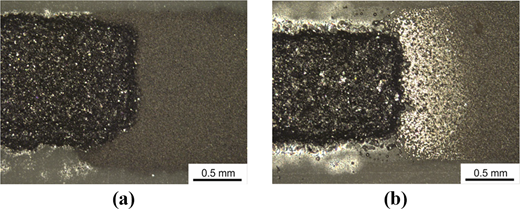
Optical image of the contact between resistor and termination layers fired in (a) air and in (b) nitrogen atmospheres
Optical image of the contact between resistor and termination layers fired in (a) air and in (b) nitrogen atmospheres
Selected samples were covered with overglaze. The samples fired in the air at 550°C were covered by QQ550 (Du Pont) overglaze and fired at the same temperature as the resistor layer. The samples fired in nitrogen atmosphere, were covered using nitrogen fireable overglaze IP7098 (Heraeus) and fired at 620°C. The results of sheet resistance measurement were shown in Table 3. Comparing the results with values for the layers without protection overglaze, the values of sheet resistance increased for samples fired in nitrogen and decreased for samples fired in the air atmosphere. The overglaze improved contact resistance between graphite grains for samples fired in the air. In contrast, the overglaze during penetration into the resistor layer deteriorated the contact between conductive grains in samples fired in nitrogen. The differences between PdAg contacts fired in air (550°C) and nitrogen (875°C) are presented in Figure 5.
Sheet resistance (RSQ) of pastes P1, P2 after covering with glaze layer
| Sheet resistance RSQ [Ω] | |||
|---|---|---|---|
| Layers | 2 | 3 | |
| Firing/glaze | Air/QQ550 | N2/IP7098 | N2/IP7098 |
| P1 | 414 ± 38 | 5.0 ± 1.5 | – |
| P2 | 167 ± 19 | 12.5 ± 2.3 | 3.6 ± 0.8 |
Assuming the effects of the glass flow, visible in Figure 5(b), the contact resistance between resistor layer and terminations were estimated from the linear fitting or resistance as a function of resistors’ aspect ratio. For direct comparison, only the four-layer resistors were considered. The results are shown in Figure 6(a) and (b) for layers fired in the air and in nitrogen atmosphere, respectively. For samples fired in the air, the resistance between two terminations and the resistor were about 760 Ω for paste P1 and about 72 Ω for paste P2. The values were high, but in relative relation to the sheet resistances, they can be acceptable. In this case, the number of conductive phase was important. For samples fired in nitrogen, the resistance of contact had higher contribution to total resistance than resistance of the resistive layer – the values of about 4 and 8 Ω were estimated. Therefore, high deviation was noticed during sheet resistance calculation for these samples.
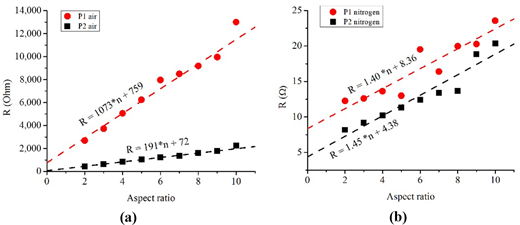
Estimation of contact resistance for resistors made of P1 and P2 fired in (a) air and in (b) nitrogen atmosphere
Estimation of contact resistance for resistors made of P1 and P2 fired in (a) air and in (b) nitrogen atmosphere
3.2 Temperature coefficient of resistance measurements
Temperature coefficient of resistance (TCR) is one of the most important parameters of resistors from application point of view. The TCR of examined resistors was calculated using the equation (2):
where is the resistance in 125°C, is the resistance in 25°C and = 100°C. Change of the pastes TCR after various technology stages were studied. Results are presented in Table 4. Because of too high standard deviation of TCR for paste P3, the measurements were rejected. The results showed that the TCR is dependent on paste composition, firing temperature and atmosphere, as well as presence of top coating glass. For Paste P1 fired in the air, the value increased after firing overglaze layer, owing to changes of microstructure, also observed as a resistance change. For paste P1 fired in nitrogen, the values were not changed after overglazing. Considering the paste P2 fired in the air, the values of TCR were almost the same – no changes of microstructure occurred, despite the resistance reduction was visible for that material and technology configuration. For the paste P2 fired in nitrogen, the values of TCR were similar for samples with two- and three-layer configuration. For the samples with four-layer resistors, the value of TCR was almost twice lower. That means the graphite grains were properly connected, and the TCR value was bringing closer to TCR of a bulk graphite, with the TCR of −280 ppm/°C (Gajewska and Pietras, 1974).
TCR values of pastes with various technology
| Paste | Firing atmosphere | Peak temperature[°C] | TCR [ppm/°C] |
|---|---|---|---|
| P1 | Air | 550 | −576 ± 22 |
| N2 | 875 | −676 ± 109 | |
| P1 overglaze | Air | 550/550 | −966 ± 25 (*) |
| N2 | 875/620 | −696 ± 86 (**) | |
| P2 | Air | 550 | −1,030 ± 14 |
| N2 | 875 | −1,060 ± 385 | |
| P2 overglaze | Air | 550/550 | −1,060 ± 12 (*) |
| N2 | 875/620 | −903 ± 21 (*) −490 ± 57 (***) |
Notes:
*Resistor layer printed twice;
**resistor layer printed three times;
***resistor layer printed four times
3.3 Influence of humidity
Humidity can influence resistor layers, especially when the layers are porous and water vapour can penetrate the material, changing the resistance. Fabricated resistors were exposed to the environment with humidity in the range from 25% to 80% RH at 40°C in a climatic chamber (Binder MKF 115). The humidity in the chamber was increased up to specified limit at time of 2 h, and the values were measured using a hygrometer. Resistance change was measured in-situ for the series of resistors on a substrate. Mean resistance change and deviation were determined for specified material and process configuration. Results are shown in Figure 7 for different samples with and without the overglaze. In case of the layers fired in air, the impact of humidity was the highest, as visible in Figure 7(a). Nevertheless, after coating by the overglaze and firing, the impact of the humidity was reduced. It means that layers fired at 550°C were porous, and an additional coating sealed the pores between the graphite grains. In a case of the resistive layers fired in nitrogen, the results depended on paste composition and the number of printed layers. For the paste P1, an additional coating reduced the impact of humidity as shown in Figure 7(b). For the paste P2, no change was observed after top coating application, as visible in Figure 7(c). Therefore, the resistors made of P2 fired in nitrogen are not required for coating with protective overglaze.
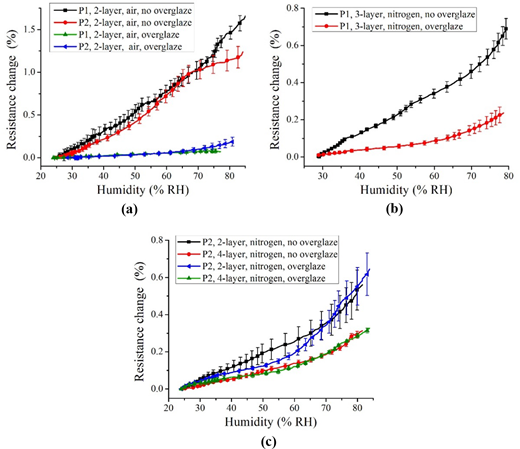
Resistance change during humidity changes for samples covered and uncovered with overglaze fired in (a) air and in (b) and (c) nitrogen atmosphere
Resistance change during humidity changes for samples covered and uncovered with overglaze fired in (a) air and in (b) and (c) nitrogen atmosphere
3.4 Short-term overload determination
Short-term overload (STOL) was determined by measurement of resistance change under consecutive load with a 5-s long electrical pulse with specified voltage. Automated setup consisting of programmable power supply and ohmmeter was used. The setup was equipped with the external switch for disconnecting the power supply from ohmmeter during the load and disconnecting the power supply from circuit for higher resistance measurement accuracy. The measurement was controlled by software working in LabView environment. STOL can be defined as an electric field intensity along the resistor, which result in resistance change of ± 1% from initial value. The parameter was determined for selected resistors with the same length for easier comparison between different material and firing atmosphere configuration. Resistance change during experiment for samples made of paste P1 and P2 are shown in Figure 8(a) and 8(b) for samples fired in air and nitrogen, respectively. In general, the overglaze on top makes the curves on the graph is changing more monotonic. Decreasing resistance in samples made of the P1 paste fired in air [Figure 8(a)] suggested a creation of new conductive paths in the microstructure, which means that the graphite grains were not properly sintered with the others. After applying and firing the overglaze, the effect was not so visible and in general, higher critical values were observed. In case of the layers fired in nitrogen, no difference was observed between coated and uncoated resistors, as visible in Figure 8(b).
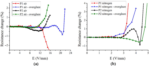
Resistance change during STOL measurement for samples fired in (a) air and in (b) nitrogen atmosphere
Resistance change during STOL measurement for samples fired in (a) air and in (b) nitrogen atmosphere
The results of STOL determination for all examined configurations are shown in Table 5. It was noticed that the parameter is dependent on the resistance of resistors – for higher resistance, the higher values of STOL parameter were determined. For direct comparison of resistors performance, a critical power density in a resistive layer at voltage corresponding to STOL values was determined. The critical power density was calculated from equation (3), where l is the length of the resistor, w is the width of the resistor and R is the resistance:
STOL for Different composition and process parameters
| Paste | Firing atmosphere | STOL [V/mm] | ||
|---|---|---|---|---|
| Two-layer | Three-layer | Four-layer | ||
| P1 | Air | 18 | 29 | 26 |
| Nitrogen | 3.2 | 2.3 | 2 | |
| P1 overglaze | Air | 21 | – | – |
| Nitrogen | – | 2.5 | – | |
| P2 | Air | 16 | 14 | 17 |
| Nitrogen | 4.7 | – | 2.5 | |
| P2 overglaze | Air | 14 | – | – |
| Nitrogen | 4.7 | – | 2.7 | |
The values of critical power density are shown in Table 6. As visible, the overglaze improves the strength of resistors fired in air, especially for paste P1. The overglaze in that case stabilised and hermitised porous structure of a resistive layer. However, no significant impact was observed for pastes fired in nitrogen because the layers were properly sintered before overglaze, and its structure was not changed during the second firing with a top coating.
3.5 Microstructure of fabricated pastes
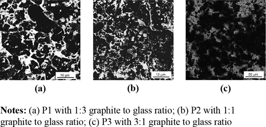
The microstructure of pastes P1, P2 and P3 after firing in 550°C (air) was studied using scanning electron microscopy (Auriga 60 Zeiss). In case of the paste P1 with the lowest contents of graphite, electric conduction was occurring probably mainly through agglomerates of the graphite surrounded by the glass material, as visible in Figure 9(b). The microstructure with non-uniformly distributed agglomerates can explain a relative high scatter of sheet resistance. The microstructure investigation revealed the best dispersion of graphite and glass phase for the paste P2 [Figure 9(b)], and thanks to that, the lowest scatter of sheet resistance and low impact of humidity were noticed. The paste P3 exhibited the highest amount of graphite, and hence the lowest sheet resistance was expected. However, as visible in Figure 9(c), the layer was porous hence the highest resistance was determined. Too low amount of the glass led to impossibility of its flow between grains, their wetting and impossible to proper densify the layer.
4. Conclusions
The novel material based on graphite-glass thick-film composition for resistive layers was presented. Applications of graphite are widely known for thick-film resistors but typically as a mix with polymers. Results of other researchers are presented in Table 7 to compare results of Rsq and TCR.
Comparison obtained layers with other researches
| Material | Rsq [kΩ/kw] | TCR [ppm/K] | Reference |
|---|---|---|---|
| Bulk graphite | 0.8* | −280 | Gajewska et al. (1974) |
| PG 10 (90% graphite) | 0.350 | 970 | Murthy et al. (1984) |
| PG 28 (80% graphite) | 0.457 | 268 | |
| PG 38 (70% graphite) | 0.718 | 406 | |
| PG 46 (60% graphite) | 2.062 | 136 | |
| 90% PVC+ 10% graphite | 45–120** | Rao (2008) | |
| MS CB EC 0.4/300 | 605 | −1,215 | Dziedzic (1997) |
| MS CB EC 0.4/350 | 200 | −1,300 | |
| MS CB EC 2/350 | 5.68 | −1,100 | |
| MS CB EC 2/300 | 3.42 | −1,000 | |
| P2 + overglaze (air) | 166.7 | −1,060 | This work – the highest |
| P2 + overglaze (N2) | 3.601 | −490 | This work – the smallest |
Notes:
*Resistivity [kΩ*cm];
**depends from grain sizes (10, 45, 70 and 100 µm)
As presented in Table 7, the most similar results of TCR are for medium size carbon black with various curing temperatures. It should be pointed out that the sheet resistance depends from grains size, type of filler and curing/firing temperature. From those results, it is hard to compare results of this research with other publications.
Low cost of materials applied for fabrication of the pastes makes them competitive to typical screen-printable pastes based on, e.g. ruthenium-oxide. Power capabilities limited to about 1 W/mm2, makes the layers suitable for the fabrication of low- and medium-power resistors in hybrid circuits. Heat from the flowing current will be not able to make significant changes of resistance. However, the constant temperature is desirable for resistors to work in high temperature. Main disadvantage of the materials is a poor repeatability of sheet resistance. Therefore, the materials are suitable for resistors without a required low tolerance of resistance. Trimming of the resistors can also be possible; however, it should be examined.
The authors wish to thank the Wroclaw University of Science and Technology (statutory activity) for financial support.

