
1-20 of 11631
Keywords: ORCUS
Close
Follow your search
Access your saved searches in your account
Would you like to receive an alert when new items match your search?
Journal

A multi-disciplinary study of technologies processes and current practices associated with miniaturized electronic devices and advanced packages.
in Development of low temperature cofired ceramics based tubes with integrated microheater for sensor applications
> Microelectronics International
Published: 20 August 2026
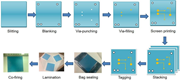
Figure 1 LTCC fabrication process flow A flow diagram shows ceramic circuit fabrication from slitting and blanking through via processing, printing, stacking, and firing. The process begins with slitting, then proceeds to blanking, where openings appear in the ceramic sheet. Via-punching cre... More about this image found in LTCC fabrication process flow A flow diagram shows ceramic circuit fabr...
in Development of low temperature cofired ceramics based tubes with integrated microheater for sensor applications
> Microelectronics International
Published: 20 August 2026
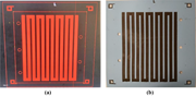
Figure 2 (a) Design layout for microheater pattern and (b) screen printed LTCC tape Two panels show a serpentine heater pattern design in panel a and its fabricated form with registration marks and input-output holes in panel b. More about this image found in (a) Design layout for microheater pattern and (b) screen printed LTCC tap...
in Development of low temperature cofired ceramics based tubes with integrated microheater for sensor applications
> Microelectronics International
Published: 20 August 2026
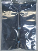
Figure 3 Bag sealed LTCC tube over mandrel LTCC tube rolled over the mandrel and sealed in a polymer bag before isostatic lamination process. More about this image found in Bag sealed LTCC tube over mandrel LTCC tube rolled over the mandrel an...
in Development of low temperature cofired ceramics based tubes with integrated microheater for sensor applications
> Microelectronics International
Published: 20 August 2026
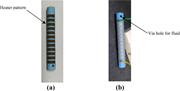
Figure 4 LTCC tube with integrated heater (a) before and (b) after firing Two panels show the fabricated device, with panel a identifying the LTCC tube with integrated heater pattern before firing and panel b identifying the LTCC tube with integrated heater pattern after firing with a via hol... More about this image found in LTCC tube with integrated heater (a) before and (b) after firing Two pa...
in Development of low temperature cofired ceramics based tubes with integrated microheater for sensor applications
> Microelectronics International
Published: 20 August 2026
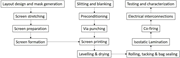
Figure 5 Fabrication flow chart for LTCC tube A flowchart shows L T C C fabrication from layout design and mask generation through processing, co-firing, and testing. The flow begins with layout design and mask generation, followed by screen stretching, screen preparation, and screen formati... More about this image found in Fabrication flow chart for LTCC tube A flowchart shows L T C C fabrica...
in Development of low temperature cofired ceramics based tubes with integrated microheater for sensor applications
> Microelectronics International
Published: 20 August 2026
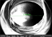
Figure 6 FESEM image of dedicated input–output hole A scanning electron micrograph shows a circular opening with a measured diameter of 2.176 millimetres. More about this image found in FESEM image of dedicated input–output hole A scanning electron microgra...
in Development of low temperature cofired ceramics based tubes with integrated microheater for sensor applications
> Microelectronics International
Published: 20 August 2026
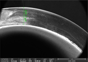
Figure 7 FESEM image depicting wall thickness of LTCC tube A scanning electron micrograph shows a curved wall section with a measured thickness of 652 micrometres. More about this image found in FESEM image depicting wall thickness of LTCC tube A scanning electron...
in Development of low temperature cofired ceramics based tubes with integrated microheater for sensor applications
> Microelectronics International
Published: 20 August 2026
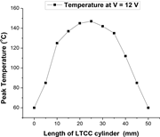
Figure 8 Temperature profile w.r.t distance over the tube A line graph shows peak temperature along a L T C C cylinder at 12 volts, rising to 147 degrees Celsius then decreasing. The horizontal axis covers L T C C cylinder length from 0 to 50 millimetres, while the vertical axis covers peak te... More about this image found in Temperature profile w.r.t distance over the tube A line graph shows peak...
in Development of low temperature cofired ceramics based tubes with integrated microheater for sensor applications
> Microelectronics International
Published: 20 August 2026
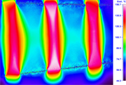
Figure 9 Thermal imaging profile of center region of the tube A thermogram shows 3 elongated heated regions with temperatures ranging from 44.3 to 150.7 degrees Celsius. More about this image found in Thermal imaging profile of center region of the tube A thermogram shows ...
Journal Articles
Journal:
Microelectronics International
Microelectronics International 1–6.
Published: 20 August 2026
Journal Articles
Journal:
Microelectronics International
Microelectronics International 1–24.
Published: 19 August 2026
in Compact electrostatic shielding devices for wide-bandgap systems with programmable microcontrollers: a review
> Microelectronics International
Published: 19 August 2026
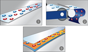
Figure 1 Illustration of static charge phenomena within electronic systems, highlighting (1) conventional static charges, (2) double-layer charges, and (3) encapsulated static charges (adapted from Aydemir et al., 2025 ), representing key electrostatic charge configurations that arise at material interfaces and within confined device structures under high electric field conditions, which are essential factors for ensuring effective compact electrostatic shielding in WBG devices Three illustrations show a charged strip passing through rollers and receiving a covering layer. The process begins in panel 1 with positive and negative charge symbols distributed across a flat strip. Panel 2 then passes the strip between rotating rollers, while a narrow blade contacts the surface and charge symbols continue along the emerging material. Panel 3 completes the process by placing a second sheet over the charged base layer, with positive and negative charge symbols retained between the layers. More about this image found in Illustration of static charge phenomena within electronic systems, highligh...
in Compact electrostatic shielding devices for wide-bandgap systems with programmable microcontrollers: a review
> Microelectronics International
Published: 19 August 2026
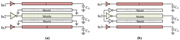
Figure 2 Comparison of shielding methods: (a) passive shielding, and (b) active shielding. The active shield induces crosstalk noise on lines 1 and 5 and exhibits higher power consumption than the passive approach due to the shield line driver (adapted from Mehri and Masoumi, 2015 ), illustrating... More about this image found in Comparison of shielding methods: (a) passive shielding, and (b) active shie...
in Compact electrostatic shielding devices for wide-bandgap systems with programmable microcontrollers: a review
> Microelectronics International
Published: 19 August 2026
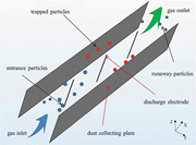
Figure 3 An illustration of the spatial arrangement of electrodes and plate configuration for compact electrostatic shielding in WBG systems, adapted from a three-dimensional model of a wire-plate electrostatic precipitator (adapted from Chen et al., 2022 ), showing how high-field regions generated by the discharge electrode and the spatial positioning of collecting plates can be conceptually mapped onto compact WBG device environments, where controlled field distribution and charge capture principles are relevant to mitigating localized electrostatic stress in densely packed power electronic modules A flow diagram traces gas and particles through discharge electrodes and dust collecting plates to a gas outlet. The gas enters with entrance particles and passes between dust collecting plates containing discharge electrodes. Some particles become trapped on the collecting plates, while runaway particles continue through the passage. The remaining gas and runaway particles then leave through the gas outlet. Axes X, Y, and Z indicate the three-dimensional orientation. More about this image found in An illustration of the spatial arrangement of electrodes and plate configur...
in Compact electrostatic shielding devices for wide-bandgap systems with programmable microcontrollers: a review
> Microelectronics International
Published: 19 August 2026
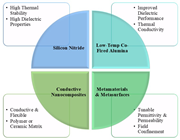
Figure 4 Key advanced materials for compact electrostatic shielding devices in microcontroller-integrated WBG systems, highlighting how each material class contributes to electrostatic shielding performance through distinct mechanisms such as dielectric insulation and thermal stability (ceramics... More about this image found in Key advanced materials for compact electrostatic shielding devices in micro...
in Compact electrostatic shielding devices for wide-bandgap systems with programmable microcontrollers: a review
> Microelectronics International
Published: 19 August 2026
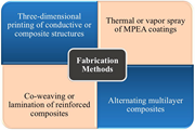
Figure 5 Key fabrication methods for compact electrostatic shielding devices in microcontroller-based WBG systems, highlighting how these techniques enable precise control over geometry, conductivity pathways, and interfacial engineering to support compact, high-density electrostatic shielding i... More about this image found in Key fabrication methods for compact electrostatic shielding devices in micr...
in Compact electrostatic shielding devices for wide-bandgap systems with programmable microcontrollers: a review
> Microelectronics International
Published: 19 August 2026
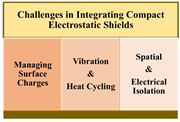
Figure 6 Key challenges in integrating compact electrostatic shielding devices in microcontroller-based WBG systems, highlighting critical barriers under high-voltage, high-frequency, and thermally demanding conditions. The challenges include surface charge accumulation and leakage control, stab... More about this image found in Key challenges in integrating compact electrostatic shielding devices in mi...
in Compact electrostatic shielding devices for wide-bandgap systems with programmable microcontrollers: a review
> Microelectronics International
Published: 19 August 2026
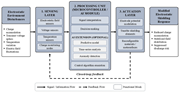
Figure 7 Conceptual block diagram of artificial intelligence-/microcontroller-driven adaptive electrostatic shielding architecture for WBG systems (AI = artificial intelligence), illustrating a closed-loop control framework where electrical, thermal, and electromagnetic interference signals are ... More about this image found in Conceptual block diagram of artificial intelligence-/microcontroller-driven...
Journal Articles
Journal:
Microelectronics International
Microelectronics International 1–11.
Published: 14 August 2026

