
Automated Bonded Wafer Inspection Tool from Sonoscan
Article Type: New products From: Soldering & Surface Mount Technology
Sonoscan has introduced the AW200™ Series C-SAM®acoustic micro imaging system (Figure 1), which performs automated inspection,analysis and sorting of bonded wafers up to 200 mm (8 in.) in diameter.
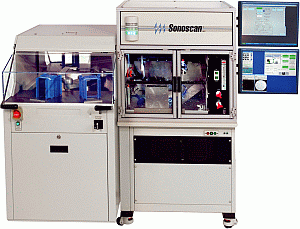
Figure 1 Sonoscan’s new AW200™ Series C-SAM® acoustic micro-imaging system
To avoid immersing the bonded wafer pair in water a technique that can conceal defects the AW200 images wafer pairs with Sonoscan's proprietary Waterfalle transducer. After imaging, the wafer pair is automatically dried.
The AW200 employs Sonoscan- designed very high-frequency transducers capable of detecting inter-wafer voids as small as 5 mm in diameter and as thin as 0.02 micron (0.0000008 in.). The transducers scan the wafer at the same high speed as other C-SAM instruments thereby providing the highest scanning throughput in the industry. The two high-precision robotic arms that handle the wafer pairs permit even higher throughput.
Automated analysis of the acoustic data accurately determines the bonded/non- bonded areas, the number and sizes of voids, zero-level package seal integrity, and the accept/reject status of the wafer pair according to the user's criteria.
For more information, please contact: Sonoscan, Inc., 2149 E. Pratt Blvd.,Elk Grove Village, IL, USA 60007. Tel.: 847 437-6400, Fax: 847 437-1550, E-mail: info@sonoscan.com,web site: www.sonoscan.com


